
News
QUANTITATIVE ANALYSIS OF FILM THICKNESSES OF MULTI-LAYER PLATING USED ON CARDS BY EDX-8000/7000
A three-layer plating of gold (Au), nickel (Ni), and copper (Cu) is often applied to the contact areas of electronic devices and IC chips. The amount of plating material deposited (film thickness) can be measured non-destructively by using X-ray fluorescence (XRF) spectrometry. This article introduces a simple quantitative analysis of Au, Ni, and Cu film of a three-layer plating by employing the thin-film fundamental parameter (FP) method without using standard samples.
Sample, Elements and Layer of Plating
1. Certified Reference Material: NMIJ CRM 5208-a, 20 mm × 20 mm
2. IC chip, SIM card
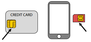
Fig. 1 IC Chip (Left) and SIM Card (Right)
3. The elements and layers of the plating are shown in Fig. 2.
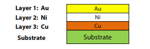
Fig. 2 Elements and Layers of Plating
Quantitative Analysis of Film Thickness
The layer of each metal, Au, Ni, and Cu, was quantitated by the thin-film FP method. The analysis diameter was set to 1 mmφ. The samples were directly set on the sample stage without any pretreatment.
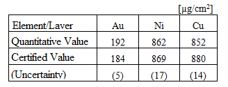
1. Certified Reference Material NMIJ
The analysis results of each layer's central point are shown in Table 1. A good result was obtained that the error of the quantitative value of each layer was within 5 % of the certified value.
Table 1 Results of the Quantitative Analysis of NMIJ CRM 5208-a
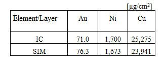
The film thicknesses analysis results of one central point on the IC and the SIM are shown in Table 2.
Table 2 Film Thickness of IC and SIM
3. Spectra
Spectra of the analytical lines of each layer are shown in Fig. 3. While the thickness of the Au layer was thin at a few dozen nm, the peak was clear, demonstrating the high sensitivity of the analysis. Standard X-ray emission lines were used for analytical lines: AuLα, NiKα, and CuKα. Kβ and Lβ lines could be used when the analytical lines of each layer's element are close to each other.
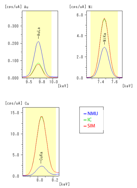
Fig. 3 Spectra of Analytical Lines
Conclusion
Film thicknesses of a three-layer plating of gold, nickel, and copper were analyzed with ease, high sensitivity and precision in the order of nm to μm using small analysis diameters of 1 mmφ and 3 mmφ. Quantitation of even thinner areas may be possible by using the standard analysis diameter of 10 mmφ. As demonstrated in this research, XRF spectrometry is effective for film thickness measurement. Furthermore, XRF spectrometry (EDX-8000/7000) can also easily analyze the elements and their amounts used in the material.
Source: ETA
Others
- TECOTEC GROUP ATTENDED SHIMADZU’S SERVICE MANAGER MEETING IN 2022
- TECOTEC HANDED OVER EDX-7000 X-RAY FLOURESCENCE SPECTROMETER AT NIDEC CHAUN CHOUNG VIETNAM
- INSTALLATION OF CHIP PROCESSING SYSTEM – LANNER/ GERMANY
- TECOTEC completed installation of EDX-LE Energy dispersive X-ray Fluorescence spectrometer at DYT Vina
- TECOTEC DELIVERED AND INSTALLED THE 2ND X-RAY FLUORESCENCE SPECTROMETER - EDX-LE PLUS AT TABUCHI
- TECOTEC Group has handed over PDA-7000 Optical Emissions Spectrometers for Nihon Plast Vietnam
- Bowman XRF Coating Measurement System For Electroless Nickel Plating
- TECOTEC DELIVERED AND INSTALLED SMX-2000 SYSTEM TO NIDEC TECHNO MOTOR VIETNAM