
News
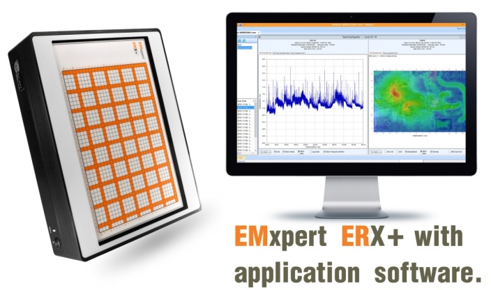
Applications EMC and EMI testing tool for PCB - EMxpert
The EMxpert provides unique pre- and post-EMC compliance testing that images emissions in less than a second. This allows the design team to immediately analyze and compare design iterations.
During any new PCB development process, design engineers must find, characterize, and address unintended radiators or RF leakage to pass compliance testing. Ideal PCB projects for the EMxpert are boards designed for high speed, high power, and/or high density/complexity. The EMxpert allows engineers to visualize the root causes of potential EMC and EMI problems.
Some examples about the applications of EMxpert patented scanner as follows:
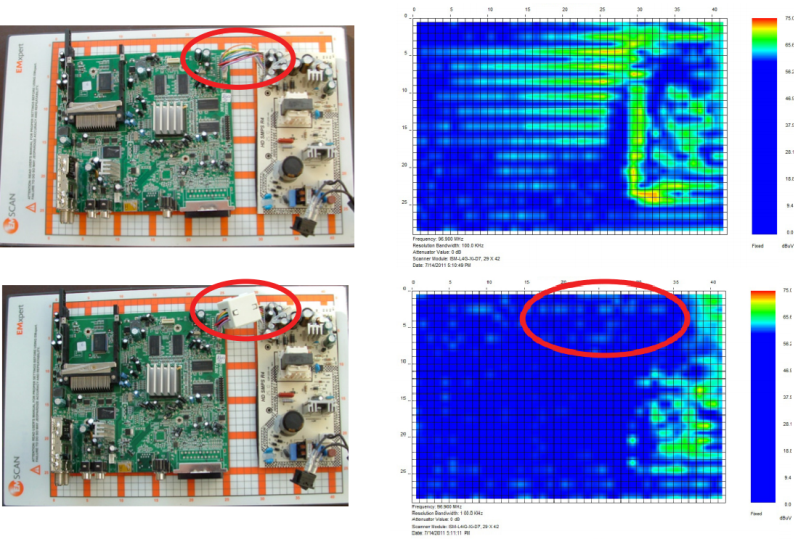
1. Determine the effectiveness of a filter in real-time
The example spatial imaging below evaluates a PCB from a satellite receiver. The device under test (DUT) is positioned on the patented scanner. The power supply is the board on the right. The image on the right above that the noise from the power supply has spread to the mother board. The emitting power supply cables are circled in red. The image on the left below shows the DUT with the red circle highlighting the filter on the cables. The image on the right below illustrates the effect of adding a filter on the cables between the power supply and the board. The noise from the mother board is completely gone, substantially improving the noise floor.
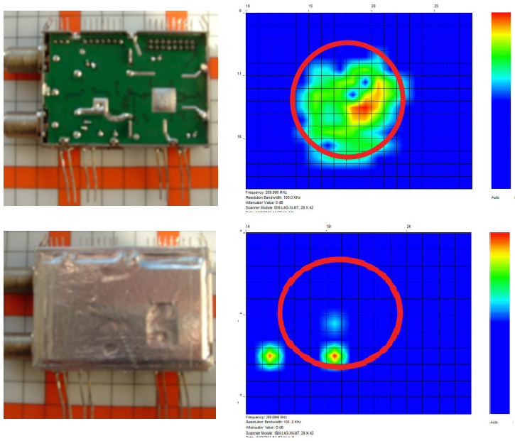
2. Shielding
EMI shielding, another noise reduction method, constrains radiating emissions. EMxpert maps very-near-field emissions generated by current flow on the board’s surface in seconds. As a result, design teams diagnose and quickly address any unexpected emission problems. The Spatial Comparison tool then facilitates immediate comparison between the shielded and unshielded solutions.
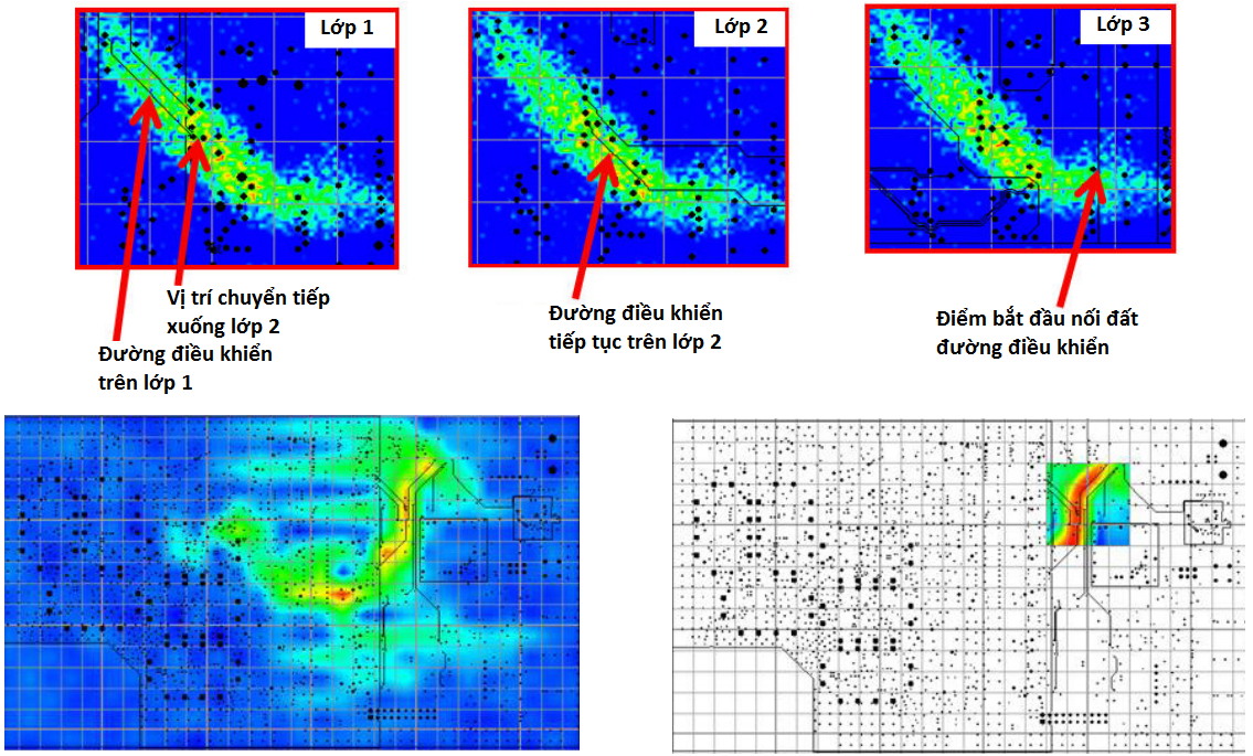
3. Identify the emission source and the path down to a single trace and via across multiple PCB layers.
The high-resolution EMxpert spatial scan available from the ERX+ gives users the ability to find the source of emissions and the path taken by the problem emissions down to a single trace and via across multiple PCB layers. An example is shown below.
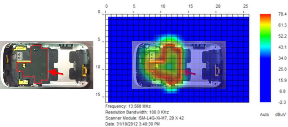
4. NFC Antenna Testing
Considering the size, frequency and distance, antenna radiation pattern is not a meaningful parameter for NFC designers. Amplitude and distribution of the signal are important. The peak-hold mode of the EMxpert can still create a full image of the antenna’s emission in seconds even with a bursty NFC signal.
In the example below a phone has a back case which comes off and exposes every antenna used for GSM, WiFi, NFC etc. The the NFC antenna section is highlighted in red. The results from the near-field scan show strong currents in an area similar to the shape of the highlighted antenna (right image below).
Source: RSI
Others
- TECOTEC GROUP ATTENDED SHIMADZU’S SERVICE MANAGER MEETING IN 2022
- TECOTEC HANDED OVER EDX-7000 X-RAY FLOURESCENCE SPECTROMETER AT NIDEC CHAUN CHOUNG VIETNAM
- INSTALLATION OF CHIP PROCESSING SYSTEM – LANNER/ GERMANY
- TECOTEC completed installation of EDX-LE Energy dispersive X-ray Fluorescence spectrometer at DYT Vina
- TECOTEC DELIVERED AND INSTALLED THE 2ND X-RAY FLUORESCENCE SPECTROMETER - EDX-LE PLUS AT TABUCHI
- TECOTEC Group has handed over PDA-7000 Optical Emissions Spectrometers for Nihon Plast Vietnam
- Bowman XRF Coating Measurement System For Electroless Nickel Plating
- TECOTEC DELIVERED AND INSTALLED SMX-2000 SYSTEM TO NIDEC TECHNO MOTOR VIETNAM