
News
ANALYSIS OF LEAD-FREE SOLDER JOINT INTERFACE
Solder joining technologies have become increasingly important in the electronics industry in recent years from the viewpoints of miniaturization of electronic components and wide adoption of lead-free solder alloys. This article introduces an example of analysis of the solder joint interface of a printed wiring board on which components were mounted with a lead-free solder alloy (Sn-3.0Ag-0.5Cu) and a crack in the solderusing a Shimadzu EPMA™ electron probe microanalyzer (EPMA-8050G, hereinafter, EPMA).
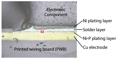
Fig. 1 - Optical Micrograph of Solder/Electroless Ni-P Plating Joint Interface
Solder/Electroless Ni-P Plating Joint Interface
In solder joints on printed wiring boards (PWB), an electroless Ni-P plating is applied on Cu electrodes. Fig. 1 shows the composition of each layer between the PWB and the electronic components mounted on the board. Fig. 2 shows the enlarged mapping results of the region in the red box in Fig. 1. This figure shows the joint interface between the solder and the electroless Ni-P plating. It can be understood that heterogenous dendritic intermetallic compounds of Ni, Cu, and Sn and a P-rich layer have formed in this region. Fig. 3 shows the enlarged mapping results for the areas in the red boxes in Fig. 2. The condition of P concentration with a thickness of several 100 nm and the distribution of fine Ag particles with size of approximately 100 nm can be captured clearly by measurement under a low accelerating voltage condition (7 kV) to reduce the spread of X-ray spatial resolution. As this example demonstrates, useful information for investigation of decreased solder joint strength and analysis of the interfacial deposition reaction process can be acquired by EPMA analysis.
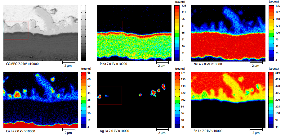
Fig. 2 - Mapping Analysis of Solder/Electroless Ni-P Plating Joint Interface
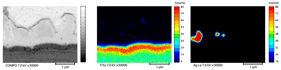
Fig. 3 - Enlarged Images of Mapping Analysis of Solder/Electroless Ni-P Plating Joint Interface
Analysis of Solder Crack
Next, a mapping analysis of an area where a crack occurred in a PWB solder joint was conducted. Fig. 4 shows the mapping analysis results. The overlay image (lower right) shows the distribution when 4 elements (Ni, Cu, Ag, Sn) were overlaid, and indicates that an intermetallic compound layer consisting of mainly Ni, Cu, and Sn has formed at the interface between the solder and the Ni plating. Focusing on the region between the intermetallic compound layer and the crack (region outlined by the red dotted line in the COMPO image at upper right in Fig. 4), it can be understood that depletion of Cu and Ag has occurred (as shown by the white dotted lines in the element distribution images for Cu and Ag in Fig. 4).
Based on these results, it can be inferred that Cu and Ag, which are originally components of the solder, dispersed and concentrated at the interface with the Ni plating layer, and the crack occurred due to the deterioration of solder strength accompanying the formation of this Cu- and Ag-depleted layer. This experiment shows that valuable information for analysis of the cause of cracks in solder joints can also be obtained by EPMA.
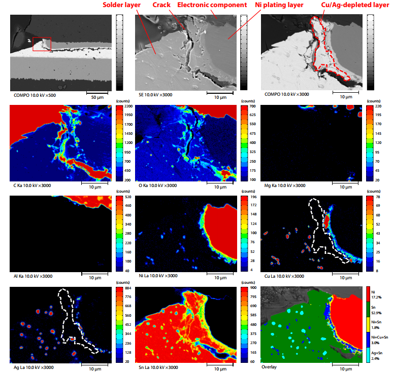
Fig. 4 - Mapping Analysis of Solder Crack
This instrument is equipped with a cutting-edge FE electron optical system, which provides unprecedented spatial resolution under all beam current conditions, from SEM observation conditions up to 1 μA order. Integration with high performance X-ray spectrometers that Shimadzu has fostered through the company's traditions achieves the ultimate advance in analysis performance. It is certainly appropriate to call this the grand EPMA, the debut of the ultimate EMPA system.
Source: ETA
Others
- TECOTEC GROUP ATTENDED SHIMADZU’S SERVICE MANAGER MEETING IN 2022
- TECOTEC HANDED OVER EDX-7000 X-RAY FLOURESCENCE SPECTROMETER AT NIDEC CHAUN CHOUNG VIETNAM
- INSTALLATION OF CHIP PROCESSING SYSTEM – LANNER/ GERMANY
- TECOTEC completed installation of EDX-LE Energy dispersive X-ray Fluorescence spectrometer at DYT Vina
- TECOTEC DELIVERED AND INSTALLED THE 2ND X-RAY FLUORESCENCE SPECTROMETER - EDX-LE PLUS AT TABUCHI
- TECOTEC Group has handed over PDA-7000 Optical Emissions Spectrometers for Nihon Plast Vietnam
- Bowman XRF Coating Measurement System For Electroless Nickel Plating
- TECOTEC DELIVERED AND INSTALLED SMX-2000 SYSTEM TO NIDEC TECHNO MOTOR VIETNAM